Dr Luis A. Pérez, Mr. Jinhui Hu, Dr M. Isabel Alonso and Prof. Alejandro R. Goñi
Institute of Materials Research of Barcelona, ICMAB-CSIC, Spain, ICREA, Spain
Mitigating the effects of global warming, primarily due to worldwide exponential growth in industrial activity and the unbound increase in greenhouse- gas emissions (mainly CO2), is just one of the major challenges facing society today. One way to contribute to this challenge is the development of sustainable energy resources to replace fossil fuels. This is where PLASMIONICO comes in.
PLASMIONICO is a European MSCA- IF project devoted to searching for alternatives to photovoltaics to harness near-infrared (NIR) solar light, which is normally wasted in conventional solar cells. The key concept is the use of purposely designed interfaces between a nanostructured metal and a semiconductor to efficiently absorb NIR solar light. The absorbed photons would then excite surface plasmons which end up injecting electrons from the metal into the semiconductor, generating a photocurrent.
The PLASMIONICO project aims to advance the sustainable production of electricity by harnessing infrared (IR) solar light, which is typically wasted in conventional solar cells.
What are plasmons?
Metals are excellent electrical conductors because they contain high densities of almost-free electrons, moving through the solid like a compressible fluid but transporting electricity. Analogous to sound waves in liquids, plasmons correspond to compressive waves of the electronic charge density. The electromagnetic field of the light readily couples to the charge carriers, transferring energy to the metal by launching plasmons at well-defined frequencies (wavelengths), so-called resonances.
In nanostructured materials, plasmons are restricted to travel along the metal interfaces; hence, they are surface plasmons. A characteristic of these surface plasmons is the extremely large enhancement of the electromagnetic field in the vicinity of the places where the electronic charge density is higher, named hot spots. The increments in charge density and consequently the field enhancements can be further boosted by nanostructuring the metal, following the lightning-rod principle. We aim to utilise these hot spots for the internal injection of electrons to produce a photocurrent.
Plasmonic nanostructures
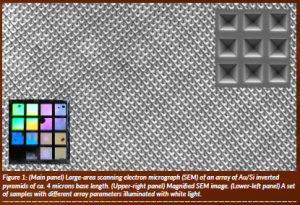
The strategy of PLASMIONICO consists of nanostructuring crystalline Si wafers in the form of perfectly ordered arrays of inverted pyramids covered with a thin gold film. The reasons for choosing silicon are twofold: it is totally transparent in the NIR spectral range, and its utilisation might allow integration of our NIR harvesters into conventional electronic devices. The transparency of Si in the infrared is crucial because inverted pyramids must be illuminated from the substrate side. In addition, we pay particular attention to employing low-cost and scalable manufacturing methods. A representative example of plasmonic nanostructures fabricated within PLASMIONICO is shown in Figure 1 for the case of an array of pyramids with a base length of ca. 4 microns covered with an Au layer of solely 50 nm in thickness. The electron-microscope image demonstrates the high quality and regularity of the pyramid arrays we manufacture (note the magnified image in the upper-right corner).
The engraved pattern also works as diffraction grating. Hence, when the inverted pyramid arrays are illuminated with white light from the top (gold side), the different colours are separated like with a prism. How strongly each colour is dispersed depends heavily on geometrical parameters such as pyramid size and/or array pitch. The colourful image in the lower-left corner of Figure 1, obtained by illuminating an arbitrary set of samples containing different pyramid arrays, illustrates how to shift plasmon resonances to the NIR spectral range simply by design.
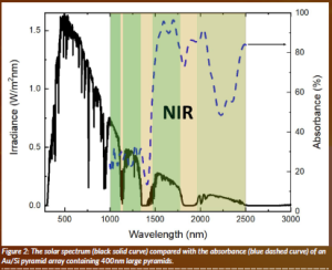
Figure 2 illustrates the results obtained from the optimisation of the inverted- pyramid array design by combining simulation and optical characterisation of the transmittance and reflectance of the ready nanostructures. The black solid curve corresponds to the wavelength- dependent spectrum of the sun, and the shaded area demarks the NIR range of interest for PLASMIONICO. The dashed blue curve represents the normalised absorbance of an array of inverted pyramids with a base length of 400nm and a slightly larger pitch (inter-pyramid separation). Apart from achieving a very high overall absorbance in the NIR, several maxima are clearly evident in the absorbance spectrum, corresponding to the plasmon resonances mentioned previously.
Photocurrent generation
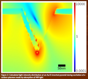
To generate a photocurrent, it is essential to visualise the distribution of the electromagnetic field in the vicinity of the metal-semiconductor interface, resulting from the resonant excitation of surface plasmons by the absorbed NIR light. Unfortunately, this cannot be measured directly but can be calculated. Figure 3 displays a typical colour plot of the field-intensity distribution along a cross-section through the middle of a pyramid, as yielded by the calculations. The bright reddish regions correspond to the hot spots, where the intensity of the incident NIR light can be amplified up to ten thousand times! It is, of course, a dynamical process and Figure 3 only shows a snapshot.
Our video visualises the entire process: arrival of the incident plane wave, excitation of the surface plasmon, several reverberations and its decay. A photocurrent arises if the surface- plasmon energy is finally transferred to electrons of the gold, injected in the semiconductor at the hot spots and collected at a counter electrode.
We have by now optimised several structures and obtained very promising results in a narrow spectral range close to the absorption edge of silicon. For inverted pyramids with several hundreds of nanometres in size, we have already attained photocurrents in excess of 1mA. The present challenge is to improve photocurrent generation for longer wavelengths as well as extending the concept to other semiconductor materials like hybrid halide perovskites and conjugated polymers. The latter is due to the possibility of developing flexible devices and hybrid perovskites, as they are revolutionising current photovoltaics due to their extraordinary optoelectronic properties.
Potential beyond clean energy
Looking ahead, we would like to point out that the mechanism of plasmon- assisted hot-electron generation studied and further developed in the framework of PLASMIONICO is not restricted to clean-energy applications. On the contrary, other research and technological areas can profit from its implementation, such as high- sensitivity detection, photo-catalysis, biological electro-stimulation, etc.
Ourgroupat ICMAB-CSIC is determined to give continuity to the research line opened by PLASMIONICO by seeking funding at the national and European level. We plan to capitalise on the gained experience to develop a novel, more efficient and scalable technology for the sustainable capture of CO₂ and its catalytic conversion into chemicals and/or fuels of industrial interest.
Figure references
Figure 1: (Main panel) Large-area scanning electron micrograph (SEM) of an array of Au/Si inverted pyramids of ca. 4 microns base length. (Upper-right panel) Magnified SEM image. (Lower-left panel) A set of samples with different array parameters illuminated with white light.
Figure 2: The solar spectrum (black solid curve) compared with the absorbance (blue dashed curve) of an Au/Si pyramid array containing 400 nm large pyramids.
Figure 3: Calculated light-intensity distribution at an Au/Si inverted pyramid during excitation of a surface-plasmon mode by absorption of NIR light.
Project summary
The PLASMIONICO project aims to advance the sustainable production of electricity by harnessing infrared (IR) solar light, which is typically wasted in conventional solar cells. The key concept is to allow IR light to be absorbed at nanostructured metal cathodes to launch surface plasmons (rapid oscillations of electronic charge analogous to sound waves in liquids) to generate a photocurrent. Our strategy uses inverted silicon pyramid arrays covered with thin gold films, manufactured employing low-cost and scalable methods. After optimising the infrared absorption performance, we are set to improve photocurrent delivery with promising results.
Project lead
Alejandro Goñi is ICREA Research Professor at the Institute of Materials Science of Barcelona, ICMAB-CSIC. He graduated in physics (Balseiro Institute, Argentina); received his PhD at Max- Planck Institute FKF, Stuttgart, Germany; and performed postdoctoral stays at AT&T Bell Labs, Murray Hill and MPI-FKF Stuttgart. He was appointed Research/Teaching Associate at the Technical University of Berlin, where he performed his Habilitation. He was awarded the Karl-Scheel Prize of the Physical Society of Berlin for his achievements in high-pressure semiconductor physics.
Project partners
The project PLASMIONICO is based at the Institut de Ciència de Materials de Barcelona, ICMAB-CSIC.
Contact details
Professor Alejandro R. Goñi
ICREA & Institut de Ciència de Materials de Barcelona ICMAB-CSIC, Campus UAB, 08193 Bellaterra, Spain
https://nanopto.icmab.es/ projects/#1559897888531- 484cb714-8842
Funding
This project has received funding from the European Union’s Horizon 2020 research and innovation programme under the Marie Skłodowska-Curie Individual Fellowship (MGA MSCA-IF) grant agreement No.839402.


