Athanasios Paralikis, Pietro Metuh, Pawel Wyborski, and Battulga Munkhbat
All from the Technical University of Denmark
Single photons (individual packets of light) hold great promise as carriers of quantum information thanks to their controllable quantum properties and their minimal interaction with the environment. They can encode information in multiple degrees of freedom and maintain coherence over long distances, making them ideal building blocks for quantum communication and computation. To unlock this potential, however, one requires a reliable single-photon source—a device that satisfies 3 key criteria. First, it must be efficient, meaning that each excitation event results in the generation of a photon. Second, it must be pure, producing 1 and only 1 photon per excitation cycle. Finally, the photons it generates must be indistinguishable, meaning they are quantum mechanically identical so that they can interfere with each other—a requirement at the heart of many quantum protocols (Gregersen, McCutcheon, and Mørk, 2017).
Developing sources that simultaneously satisfy all 3 criteria remains one of the central challenges in modern quantum science. Although remarkable demonstrations already exist, turning these early successes into practical, scalable technologies is far from trivial.
One promising route forward, as far as scalability is concerned, is on-chip photonic integration. By embedding single-photon emitters directly into photonic circuits, photons can be generated, manipulated, and detected on a single platform. This approach enables compact and stable architectures, while also being compatible with established semiconductor fabrication techniques. In effect, if the early history of quantum optics emphasised mastering isolated quantum systems, the future will revolve around integration and scalability—bringing coherent quantum light into practical devices (Wang, 2020).
Within this context, two-dimensional materials, and especially transition metal dichalcogenides (TMDs), have emerged as compelling candidates for quantum light generation. When thinned down to a monolayer, some of these semiconductors emit light efficiently across a wide spectral range, from the visible to the telecom bands. Their atomic thickness offers unique advantages as they can be transferred onto nearly any substrate, patterned into desired geometries, and combined with other 2D materials to form designer heterostructures. These features make TMDs naturally compatible with photonic and electronic platforms, providing a clear route toward scalable quantum photonic systems (Montblanch, 2023; Esmann, 2024).
Our group focuses on leveraging this versatility to create reliable, high-quality single-photon sources while systematically addressing the key challenges that limit their performance. Our efforts span both fabrication—developing reproducible methods that produce emitters with high yield and controlled properties—and advanced optical characterisation, which helps us understand and mitigate the subtle mechanisms that degrade coherence and stability.
Developing a reliable fabrication method
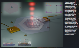
A major component of this work has been establishing a reproducible fabrication process that also overcomes 3 longstanding challenges in TMD-based emitters. The first is gaining reliable control over the location of the emitters, which is essential for integrating them with photonic structures. The second is maximising the yield of emitters per device, which greatly accelerates experimental progress. The third— and crucial for photonic coupling— is controlling the orientation of the emitter’s linear polarisation. By making use of nanostructures with non-trivial geometries (Figure 1), we managed to achieve all 3 goals. These structures create oriented nanowrinkles whose ridges define a one-dimensional strain profile. When combined with controlled introduction of lattice defects using high-energy irradiation, these strained regions consistently produce single-photon emitters with reproducible polarisation directions (Paralikis, 2024).
Reducing charge noise: a major decoherence factor
Our second line of investigation focuses on mitigating charge noise, one of the most significant limits to photon indistinguishability. Charge noise stems from fluctuating charges in the environment and can broaden the emission spectrum by several orders of magnitude more than phonons (Vannucci, 2024). To address this issue, we explored 2 strategies widely used to stabilise emission: passive encapsulation and active electrical biasing, the effects of which are shown schematically in the bottom-left inset of Figure 1.
In the passive approach, the TMD flakes are encapsulated in hexagonal boron nitride (hBN), a clean and stable dielectric material that isolates them from charge fluctuations in both the substrate and the environment. Encapsulation alone resulted in striking improvements, including narrower linewidths, single-exponential decay curves, and more stable emission over time—clear signatures of reduced charge noise. The active approach, applying a bias across the TMD heterostructure, proved effective only when combined with encapsulation. Under these conditions, we observed resolution-limited linewidths and remarkably stable emission, suggesting that residual noise may now lie below our detection threshold. Biasing also allowed precise control of the emission wavelength via the linear Stark effect. To bring greater consistency to the field, we proposed 2 figures of merit that quantify how close an emitter operates to the transform-limited regime, helping benchmark progress across studies (Paralikis, 2025).
Tailored excitation schemes
The third direction of our research examines how best to excite TMD emitters, since the excitation scheme plays a decisive role in determining photon coherence. Standard above-band excitation, though commonly used, generates unwanted charge carriers and promotes complex relaxation pathways that degrade indistinguishability. Fully resonant excitation, while optimal in principle, is experimentally demanding due to the limited collection efficiency imposed by the cross-polarisation setup needed to filter out the pump laser.
To navigate between these extremes, we systematically compared 3 pulsed excitation schemes—above-band, near-resonant, and phonon-assisted—on bilayer WSe₂ emitters, as shown in the top-right inset of Figure 1. Complementing this experimental study, we developed a theoretical model that captures the coupling of the emitter to its phonon environment. In addition to the longitudinal acoustic (LA) phonons found in both monolayers and bilayers, bilayer systems host unique shear (SM) and breathing (BM) modes that depend sensitively on the interlayer spacing. Our model predicted that LA phonon-assisted excitation could populate the exciton state with efficiencies exceeding 80 % at moderate detuning, and that the BM mode provides an additional excitation pathway at larger detuning.
Guided by these predictions, we demonstrated LA phonon-assisted excitation experimentally, achieving a twofold reduction in spectral diffusion compared to above-band pumping. By exploiting BM-assisted excitation—which operates at even larger detuning and therefore provides full suppression of the laser background—we performed single-photon measurements with an order-of-magnitude reduction in lifetime and a significantly narrowed linewidth. These observations indicate that phonon-assisted schemes can deliver high coherence while avoiding many limitations of resonant excitation (Piccinini, 2025).
Towards telecom-range single-photon sources
The final part of our work expands the accessible wavelength range of TMD-based emitters through a systematic study of single-photon emission from bilayer MoTe₂, which naturally emits in the near-infrared and can reach wavelengths around 1200 nm. Having
identified the importance of reducing substrate-induced noise, we fabricated our best devices on a distributed Bragg reflector (DBR) substrate. A DBR is essentially a simple stack of alternating materials engineered to strongly reflect light within a specific wavelength range, thereby enhancing the amount of light we can collect from the emitter. Placing the MoTe₂ flake directly on the DBR and capping it with a thin Al₂O₃ layer increased the brightness of the emitters while maintaining a clean and stable dielectric environment. To evaluate reproducibility, we also fabricated emitters on standard Si/SiO₂ substrates, confirming that our methods remain robust without relying on specialised optics.
Our optical characterisation compared above-band and quasi-resonant excitation, where the latter provided narrower linewidths and simpler mono-exponential decay curves, consistent with reduced charge generation. We further explored the roles of hBN encapsulation and electrical biasing. While the improvements were less dramatic than those seen in WSe₂—a result of the already optimised substrate design—these measurements revealed valuable insights into the strain landscape of bilayer MoTe₂, including clear observations of fine-structure splitting that correlate with engineered strain. Electrical biasing proved especially powerful, offering nearly ±3 nm of wavelength tuning and noticeable reductions in lifetime and charge-induced dephasing.
This work culminated in a measurement of the current state-of-the-art indistinguishability for TMD-based quantum emitters, reaching values around 10 %. This represents a fivefold improvement over previous demonstrations and marks only the second report of measurable indistinguishability in this material system. Although this performance remains below that of more mature solid-state platforms, it represents a clear milestone: strong evidence that TMD emitters are rapidly improving and that deterministic, indistinguishable single-photon sources operating near the telecommunications range are within reach (Wyborski, 2025).
Beyond source development, our group is now working toward the complementary components required for a fully integrated quantum photonic platform. This includes the realisation of waveguides, beam splitters, and even single-photon detectors (Metuh, 2025)—all based on the same 2D material platform. By fabricating every key element using TMDs, we move closer to the vision of a fully integrated, on-chip quantum optical network where light is generated, guided, and detected within a unified and scalable architecture.
References
Esmann, M., Wein, S.C., and Antón-Solanas, C. (2024). ´Solid-state single-photon sources: recent advances for novel quantum materials’, Advanced Functional Materials, 34(30), 2315936. Available at: https://doi.org/10.1002/adfm.202315936.
Gregersen, N., McCutcheon, D.P.S., and Mørk, J. (2017) ‘Single-photon sources’, in Piprek, J. (ed.) Handbook of Optoelectronic Device Modeling and Simulation. CRC Press, pp. 585–608.
Metuh, P. et al., (2025). ´Toward single-photon detection with superconducting niobium diselenide nanowires´. ACS Photonics, 12(11), pp. 5912–5920. Available at: https://doi.org/10.1021/acsphotonics.5c01195.
Montblanch, A.R.P. et al., (2023) ´Layered materials as a platform for quantum technologies´, Nature Nanotechnology, 18(6), pp. 555–571. Available at: https://doi.org/10.1038/s41565-023-01354-x.
Paralikis, A. et al., (2024) ´Tailoring polarization in WSe2 quantum emitters through deterministic strain engineering´, npj 2D Materials and Applications, 8(1), 59. Available at: https://doi.org/10.1038/s41699-024-00497-2.
Paralikis, A. et al., (2025) ´Tunable and low-noise WSe2 quantum emitters for quantum photonics´, PRX Quantum, 6(4), 040339. Available at: https://doi.org/10.1103/cynh-ql3j.
Piccinini, C. et al., (2025) ´High-purity and stable single-photon emission in bilayer WSe2 via phonon-assisted excitation´, Communications Physics, 8(1), 158. Available at: https://doi.org/10.1038/s42005-025-02080-7.
Vannucci, L. et al., (2024) ´Single-photon emitters in WSe2: Critical role of phonons on excitation schemes and indistinguishability´, Physical Review B, 109(24), 245304. Available at: https://doi.org/10.1103/PhysRevB.109.245304.
Wang, J. et al., (2020) ´Integrated photonic quantum technologies’, Nature Photonics, 14(5), pp. 273–284. Available at: https://doi.org/10.1038/s41566-019-0532-1.
Wyborski, P. et al., (2025) ´Toward triggered generation of indistinguishable single-photons from MoTe2 quantum emitters´, DTU Department of Electrical and Photonics engineering. Unpublished.
DISSEMINAT
TMD-based single-photon sources for quantum photonics
PROJECT SUMMARY
TMD-based single-photon sources for quantum photonics (TuneTMD) focuses on developing atomically thin single-photon emitters for optical quantum information processing. Its aim is to uncover the physical mechanisms behind these emitters while improving both their fabrication and their optical performance. So far, the project has established a deterministic and reproducible fabrication process, provided a clear experimental pathway to low-noise and resolution-limited emission, and demonstrated the advantages of advanced excitation schemes. It has also expanded the usable emission range toward the near-infrared while achieving state-of-the-art indistinguishability for this material platform. Looking ahead, the goal is to integrate these emitters with other TMD-based optical components to move toward a fully functioning, on-chip quantum optical network.
PROJECT LEAD PROFILE
Battulga Munkhbat is an associate professor at the Technical University of Denmark and project lead with expertise in quantum nanophotonics and 2D materials. He received his PhD in photonics from Johannes Kepler University Linz and was a postdoctoral researcher at Chalmers University of Technology, Sweden, before his current position in Denmark. He is the recipient of an ERC Starting Grant and a Villum Young Investigator Grant, and leads interdisciplinary projects developing scalable quantum photonic hardware, including single-photon sources and ultra-fast detectors, targeting future photonic quantum information technologies.
PROJECT CONTACTS
Lead researcher
Associate Professor Battulga Munkhbat
Email: bamunk@dtu.dk
LinkedIn: /in/battulga-munkhbat-b8b053118/
Dr Pawel Wyborski
Email: pawyb@dtu.dk
LinkedIn: /in/pawel-wyborski
Pietro Metuh
Email: piemet@dtu.dk
LinkedIn: /in/pietrometuh
Athanasios Paralikis
Email: athpa@dtu.dk
LinkedIn: /in/athos-paralikis
FUNDING
This project has received funding from the European Research Council (ERC) under the European Union’s research and innovation programme (Grant agreement No. 101076437).
Funded by the European Union. Views and opinions expressed are, however, those of the author(s) only and do not necessarily reflect those of the European Union or the European Research Council. Neither the European Union nor the granting authority can be held responsible for them.
Figure legends
Figure 1: Schematic representation of a fully encapsulated TMD single-photon emitter in contact with a gold electrode. The top-left inset showcases a TMD flake resting on top of a star-like nanopillar, generating the desired nanowrinkles with controlled orientation. The bottom-left inset is directly reprinted from Paralikis, A., et al. (2025) and showcases the effect of the two strategies used to minimise charge noise in the emitters. The top-right inset is a schematic representation of a trivial above-band excitation strategy versus a non-trivial phonon-assisted excitation strategy.